Safe Waste Gas Abatement in High-Tech Industries
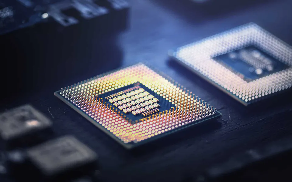
The manufacture of powerful high-tech products like microchips, photovoltaic modules, flat screens, and Light Emitting Diodes (LEDs) requires highly complex, multistage manufacturing processes. Each production sub-step creates waste gases that have to be abated directly at their point of origin (Point-of-Use).

Reliable Waste Gas Abatement at the Point-of-Use
At DAS Environmental Expert our systems are as flexible and unique as our clients. Currently we offer waste gas abatement technology in four process groups: The combination of burner and scrubber in one system is DAS Environmental Expert’s specialty. The ESCAPE and STYRAX systems are part of this product group. The LARCH product family is used for process waste gases with high hydrogen content. The gas scrubbers of the AQUABATE product group and SALIX gas scrubbers wash harmful water-soluble substances from process waste gases.
The electrostatic dust collectors of the EDC product line utilize an electrical field to remove fine particles (micro and nanoparticle) from waste gases. The electrostatic condensate separators of the JUNIPER series use the same principle to intercept and remove Volatile Organic Compounds (VOCs) from exhaust streams. DAS Environmental Expert cultivates a close collaboration with its clients. We provide cost-effective processes for reliable and safe waste gas abatement, and we develop and enhance our systems. When a client’s technologies change, we adapt and adjust our waste gas technology according to the client’s needs.
CVD/MOCVD
Chemical Vapor Deposition (CVD) deposits thin films onto substrates via a gas-phase chemical reaction. If a metal-organic compound is used, it is called Metal-Organic Chemical Vapor Deposition (MOCVD).
CVD processes produce precise thin films from metals, silicon nitride, silica, and polysilicon and rely on gases like silane, ammonia, TEOS, or nitrogen trifluoride. DAS Environmental Expert’s UPTIMUM and STYRAX product lines are tailored for CVD waste gas treatment. MOCVD is used in the semiconductor sector and for Light Emitting Diode (LED) manufacturing, where hydrogen- and ammonia-containing exhaust gases must be treated. For these, DAS has developed the LARCH Point-of-Use system to abate large process gas volumes.
TCO
In recent years Transparent Conductive Oxides (TCO) have gained large economic significance. These translucent thin films are important components of flat screens and thin film solar modules; the thin films are manufactured through thermic evaporation or specific CVD processes. Large amounts of the waste gases resulting from these processes can be abated directly at Point-of-Use through the burner-scrubber technology featured in the UPTIMUM system.
Etching
Etching ablates material from a surface by means of corrosive substances. Because it is characterized by high precision, the process is used particularly in the semiconductor industry and for the manufacturing of Micro Electrical Mechanical Systems (MEMS). Non-ablated structures are protected from the chemical etching through a specific photoresist. The chip manufacturing industry uses both wet chemical and dry etching processes, such as plasma etching and reactive ion etching. The waste gases resulting from these processes typically contain diverse fluorine compounds. The burner-scrubber technology of DAS Environmental Expert ESCAPE and STYRAX product lines efficiently treat these process waste gases.
Epitaxy
The semiconductor industry uses epitaxy to deposit crystalline films or overlayers onto a carrier substrate. The layers are characterized by their high purity and can be doped with a better precision than common doping methods. The films are manufactured either through specific chemical and physical vapor deposition processes, their hybrid forms, or with liquid-phase epitaxy. The waste gases from these processes can contain hydrogen, dichlorosilane, and germane. The DAS Environmental Expert scrubbers of the AQUABATE product line and the burner-scrubbers of the ESCAPE and STYRAX line provide safe and reliable abatement options, according to waste gas contents.
Wafer Cleaning
Following certain production steps, semiconductor manufacturing requires wafer cleaning. To accomplish this, chip manufacturers, especially those of 300 mm wafers, use single wafer cleaning. The process spins individual wafers at high speed and wets them with cleaning liquids.
Depending on the wafer’s impurities, various cleaning methods apply acidic or alkaline chemicals or solvents like acetone, ethanol, and isopropyl alcohol. After each cleaning step, the disks are rinsed with ultrapure water and dried residue-free.
The cleaning agents produce exhaust containing gaseous or droplet residues. The gas scrubber SALIX from DAS Environmental Expert reliably vacuums and purifies these contaminated exhausts.
VOC
Carbonaceous compounds that easily evaporate are called Volatile Organic Compounds (VOC), with some compounds that evaporate to a gaseous state at room temperature. Both the semiconductor and solar industries use such substances as auxiliary materials. VOC often have an unpleasant odor and can be toxic and harmful to the environment.
VOC emissions can also cause substantial damage to the manufacturing plant. When VOC condensate in exhaust systems, the condensate can escape through leaks and pose a health risk to employees, or flow back into the manufacturing systems and cause fires. DAS Environmental Expert designed the system JUNIPER to avoid such risks, and safely remove these hydrocarbons from the exhausts of manufacturing plants.
Particulate Matter
Many waste gas abatement processes require dust extraction. Dusts from waste gases are fine solid particles that can remain suspended in air for extended periods. Particles larger than ten micrometers are considered coarse dust and are caught by nasal hairs or mucous membranes. Dusts of particles smaller than ten micrometers (PM10) are called particulate matter and, if inhaled, can reach deep into the lungs.
Particles smaller than 2.5 micrometers are called fine particles (PM2.5), and those below 0.1 micrometers ultrafine particles. These micro particles are difficult to treat because they often pass through gas scrubbers or separators without being captured.
DAS EE developed the electrostatic dust collector EDC product line to reliably collect such particulate matter. EDC systems are used in the semiconductor, solar, and flat screen industries and ensure compliance with strict emission limits, particularly for arsenic in LED manufacturing.
Consulting and Technology Selection
The selection of the appropriate technology is carried out by our application specialists after analyzing the situation on site. Information about the process tool, vacuum pump, gas types and flows as well as the available operating materials are decisive.
In order to ensure a long-term runtime and tool availability, our service and technical support are available on demand or on-site as soon as the system is commissioned.
Director Key Account Management Global


